Thin film deposition - TFD
Album
Thin film deposition 1
Thin film deposition 2
Short description
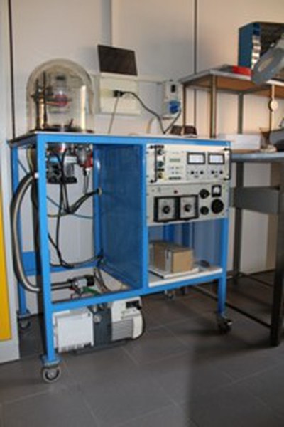
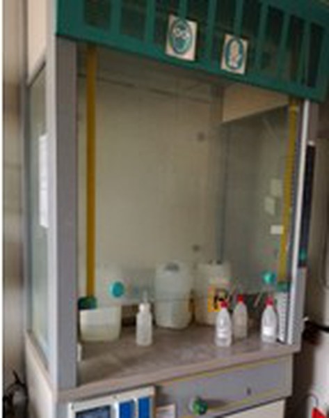
It is a laboratory where research and teaching activities are carried out, at the level of the bachelor and master's degree in Physics. Vapor phase metal elements are deposited on semiconductor surfaces for making contacts in vacuum. Semiconductor samples are also prepared: surface preparation, cutting, surface lapping, chemical etching under chemical hood. In the laboratory there are: vacuum systems (rotary pump, turbomolecular pump), instruments for the preparation of samples and surfaces (diamond saw, lapping machine), chemical hood and cabinet to contain solvents and acids for chemical etching.
Research themes
- Analysis of defects in silicon
- Analysis of defects, interfaces and surfaces in semiconductors III.N
- Analysis of defects, perovskite surfaces
Instrumentation
- Vacuum systems (rotary pump, turbomolecular pump)
- Chemical hood
- Wire saw
- Lapping system
Teaching and training
The IVD laboratory offers its resources to support:
- Thesis development (LM in Physics, MANO curriculum)
- Development of research projects for PhD students and postdoctoral students
Responsible
Beatrice Fraboni
Full Professor